Trapping the Light Fantastic
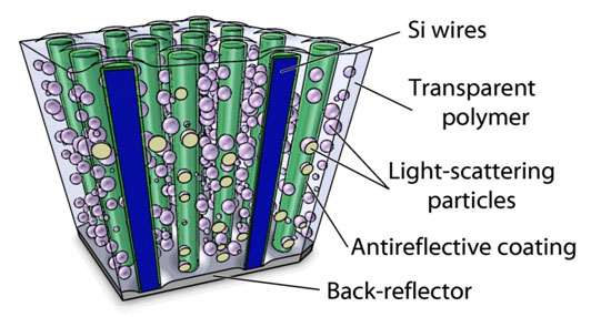 Image courtesy of California Institute of Technology
Schematic of Atwater team’s silicon nanowire solar cell.
Major advances in the understanding of light have punctuated the history of modern physics—from Newton's 1740 classic Opticks to Einstein's landmark 1905 paper on the photoelectric effect, demonstrating the particle nature of light (what today we call "photons") and ultimately earning Einstein the Nobel Prize. Today the focus of optics is increasingly on light's behavior at the nanoscale, where interactions among photons, electrons, and mysterious quasi-particles called plasmons define a whole new world as rich in complexity as it is miniscule. This world holds out more than mere theoretical interest for physicists. Probing it may be one key to making solar energy truly economically viable as a major renewable energy source in the coming years.
One of the more promising new applications of such nano-optics to solar energy is the work of Harry Atwater and his team at the California Institute of Technology. Starting with a focus on harvesting and trapping light, Atwater's group has developed an entirely new design for a thin-film silicon solar cell, which promises to achieve efficiencies rivaling today's top-of-the-line commercial silicon cells, at potentially a fraction of the cost. If successful, the technology could help take us a step closer to "grid parity," the long-sought-after point at which solar photovoltaics become inexpensive enough to be genuinely cost-competitive with fossil fuel-generated electricity. In the space of a year, Atwater's unusually promising design has gone from the lab bench to the early stages of commercialization, aided by a $1 million incubator grant from the Department of Energy and a newly raised round of venture capital.
The story illustrates not only how insights from very fundamental science can transform energy technologies. It also shows how research integration and teaming can accelerate both discovery and the transition from discovery to innovation.
Atwater leads one of 46 Energy Frontier Research Centers (EFRCs) established in 2009 at universities, national laboratories, and other institutions by the DOE Office of Science, in an effort to accelerate energy research by enabling scientists to forge multi-institutional, highly motivated teams. The EFRC grants—ranging from $2-5 million per year for an initial five-year period—provide somewhat larger and longer-term funding than is typical for grants to encourage team-building and facilitate stronger collaborations. Atwater's EFRC, appropriately named "Light-Matter Interactions in Energy Conversion," has brought together leading scientists from three powerhouse materials science institutions: the Department of Energy's Lawrence Berkeley National Laboratory, the University of Illinois, and Caltech, where Atwater is also Howard Hughes Professor and Professor of Applied Physics and Materials Science.
Atwater and his team represent a new breed of scientists who are working at the nexus of fundamental discovery, technology, and economics. Atwater's group is applying some of the most profound insights of present-day optics to a simple techno-economic problem: making a cheaper, better solar cell.
Solar cells have actually declined fairly steadily in cost over the past decades—though most experts would probably agree that grid parity remains some years away. One of the more important recent developments has been the emergence of thin-film silicon cells, which are much less expensive to fabricate than traditional crystalline silicon cells, and which represent an ever-increasing share of the growing solar cell market.
The one drawback of the thin-film cells is that they are only about half as efficient as crystalline silicon at transforming sunlight into electricity. According to the U.S. Energy Information Agency, the highest quality single-crystal silicon cells, made in wafer form, today achieve energy conversion efficiencies of up to 20 percent, while the efficiency of amorphous (i.e., non-crystalline) silicon thin-film cells hovers around 8 percent. (Some other types of wafer-based silicon cells have values in the mid-range between the two.) That's one reason why home solar systems generally use the more expensive crystalline cells—there's not enough room on the average home roof for the thin-film variety, which generate less electricity per area of exposure to the sun.
In part, the weakness of the thin-film cells lies in their very thinness.
One of the most important values in determining the efficiency of a solar cell is simply the percentage of light that the semiconductor material is able to absorb—particularly in the "usable" frequencies in which the semiconductor converts light to electricity. Manufacturers of wafer-based silicon cells typically drive up efficiency by making the cell in a wafer thick enough to trap most of the photons and enhance their absorption by the silicon. But this approach adds to both material and fabrication costs.
In 2009 Atwater and his colleagues set out to discover how nanostructures with special electromagnetic properties embedded in the thin-film cell might be able to scatter and redirect light so as to trap light longer in the film, enabling more photons to be absorbed by the semiconducting silicon. (Imagine a pinball machine with a handful of pinballs—representing photons of light—ricocheting around the bumpers over and over again.) It was highly theoretical work involving the precise tracking of various kinds of resonances—including so-called plasmonic resonances, which result from subtle vibrations of electrons on the surface of metals—across nanometer distances. Much of the complexity derives from the fact that the nanostructures are actually smaller than the wavelength of visible light. Still, the relationships are fairly well-defined mathematically.
The researchers' work on plasmonic solar cells, which predated the EFRC award, inspired them to think about other kinds of light trapping structures that could enhance absorption in silicon solar cells. The EFRC award enabled the team to direct their discovery efforts to another type of silicon solar cell structure, and then they hit upon an ingenious design. Instead of fashioning the thin film wholly out of a wafer or film silicon, as is typically done, they borrowed an idea from other work in nanoscience and fabricated a forest of silicon nanowires—tiny, ultra-thin wires of highly crystalline silicon—using a well-known laboratory technique called vapor-liquid-solid growth. This is a fairly rapid technique by which such wires can be synthesized in a reactor chamber.
Initially, the researchers spaced the wires fairly close together. But first through the use of theory and computer simulations, and later via experiments, they found better results from spacing the wires farther apart. Drawing on their earlier research, they interspersed between the wires nanoparticles specifically designed to help scatter and trap light, ultimately enabling the semiconductor wires to absorb more photons. The whole wire array structure is embedded in a flexible, transparent polymer with a reflective backing.
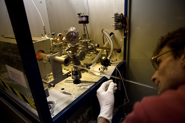 Photo by Dave Bullock
Morgan Putnam of the Atwater team inserts wafer into reactor where silicon nanowires will be grown.
Using this approach, the researchers were able to achieve a wire array solar cell with 95 percent light absorption, 9 percent conversion efficiency, approximately 600 millivolt open-circuit voltage (a respectable level), and something called an 80 percent "fill factor." The last variable—a very important measure of the commercial quality of semiconductor solar cell material—has to do with the simultaneous maximum combination of voltage and current at which the cell can operate. Seventy percent is usually the minimum cutoff for commercially sold cells.
But the final breakthrough lay in achieving this result using only 1 percent of the silicon normally used in a thin-film cell. "Our approach allows you to eliminate silicon wafer consumption," said Atwater, "one of the key costs in manufacturing solar cells."
Since silicon accounts for about 50 percent of the cost of the cell, the approach represents an enormous opportunity for potential manufacturing savings. In addition, researchers have shown that with a combination of more sophisticated modeling of the light trapping, along with improvements to the silicon's semiconductor photovoltaic properties through well-known industrial techniques, they would likely to be able to raise conversion efficiencies to 17 percent—a level competitive with the much more costly crystalline silicon cells.
So the promise, then, is of a thin-film cell measurably cheaper to produce than current thin-film silicon cells and with performance nearly comparable to the much more costly crystalline silicon cells that now dominate the market. The achievement earned Atwater and his team a Breakthrough Award from Popular Mechanics in 2010.
As an additional advantage, the flexible, thin-film structure will potentially make the cells much cheaper and easier to deploy. As Atwater told Popular Mechanics, the cells "have the optical and electronic properties of conventional solar cells but the mechanical properties of a plastic bag."
Today the effort continues on two tracks. First, Atwater and his collaborators formed a start-up company called Caelux to explore commercial scale-up of the technologies. Caelux has been awarded an incubator grant by DOE's Photovoltaic Solar Incubator Program managed by the Department's Office of Energy Efficiency and Renewable Energy. Along with the DOE grant, the company has raised venture capital. Among its first efforts will be to explore whether the vapor-liquid-solid growth technique, widely used in laboratories around the world, will scale up as a commercial technology.
Within the EFRC, Atwater and his fellow researchers continue to explore better methods of trapping light for solar cell production—and the fundamental limits of these approaches—and have plans to develop a series of alternative designs. The work involves a combination of material fabrication and characterization along with computational simulation, relying on computational resources both at Caltech and Berkeley Lab's National Energy Research Scientific Computing Center. And it's only one of several research projects in the works at the EFRC.
Atwater notes that the EFRC funding—by providing greater resources and facilitating closer and more sustained collaboration among researchers—was critical to the unusually rapid advances the researchers were able to make, from concept to lab bench prototype to initial steps toward commercialization. "The intellectual base provided by the EFRC allowed us to make pretty rapid progress," he said. "We were able to show, starting with the science of light scattering, that this design was going to have the same efficiency as much more expensive silicon cells, and to do so within the space of a year."
—Patrick Glynn, DOE Office of Science, Patrick.Glynn@science.doe.gov
Funding
Research (EFRCs): DOE Office of Science, Office of Basic Energy Sciences
Facility (NERSC): DOE Office of Science, Office of Advanced Scientific Computing Research
Selected Publications
M. D. Kelzenberg et al. "High-performance Si microwire photovoltaics," Energy & Environmental Science 4 866 (2011)
M. D. Kelzenberg, "Enhanced absorption and carrier collection in Si wire arrays for photovoltaic applications," Nature Materials 9 239 (2010)
P. N. Saeta et al. "How much can guided modes enhance absorption in thin solar cells?" Optics Express 17 20975 (2009)